Why Elon Musk Committed $119B to Terafab ── Inside the $600M High-NA EUV Bottleneck, NVIDIA's $366B Supply Lock, and Japan's 10 Chokepoint Suppliers
With frontier artificial intelligence compute demand tripling annually against an 18-month equipment lead time cap and ASML’s sub-100 EUV output, SpaceX and Tesla are attempting vertical fab integration while NVIDIA locks $366 billion in wafer and HBM capacity.
Published: October 26, 2026 | Read time: ~10 min | Watch Video (Japanese)
Executive Summary & Core Physical Constraints
In October 2026, technology journalist Dwarkesh Patel published an investigation inside Intel’s Fab D1X in Hillsboro, Oregon, interviewing Intel CTO Pushkar Ranade and process development lead Chris Auth. Correlating their insights with Texas Chapter 403 tax dockets, SpaceX’s Form S-1, and NVIDIA’s SEC filings reveals the true driver behind Elon Musk’s multi-phase $119 billion megagab, TeraFab AI, LLC:
Terafab is not an effort to reduce unit costs. It is an existential commitment driven by the reality that even unlimited capital cannot purchase sufficient leading-edge wafers, high-bandwidth memory (HBM), or advanced packaging from merchant foundries (TSMC and Samsung) over the 2026 to 2030 cycle.
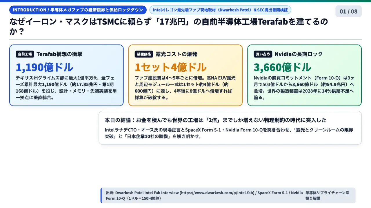
Frontier AI model training clusters and autonomous robots demand compute expansions tripling (3x) annually, but three physical barriers cap supply:
- The 2x Global Output Cap: ASML produces fewer than 100 extreme ultraviolet (EUV) scanners annually due to optical limits at Carl Zeiss SMT. With wafer fab equipment (WFE) lead times averaging 18 months, leading-edge wafer output cannot expand by more than 2x annually regardless of capital deployed.
- NVIDIA’s $366 Billion Preemptive Lock: Between October 2025 and July 2026, NVIDIA expanded binding purchase obligations from $50.3 billion to $366.0 billion, locking foundry runs, HBM lines, and chip-on-wafer-on-substrate (CoWoS) packaging through 2028.
- Equipment Supply Deficit: Surging HBM manufacturing consumes roughly three times the equipment and floor space per gigabit compared to standard DRAM, pushing the WFE market toward $281 billion by 2028 and creating a structural 14% hardware equipment shortfall.
1. Technical Baseline: High-NA EUV, HBM Density, and Purchase Obligations
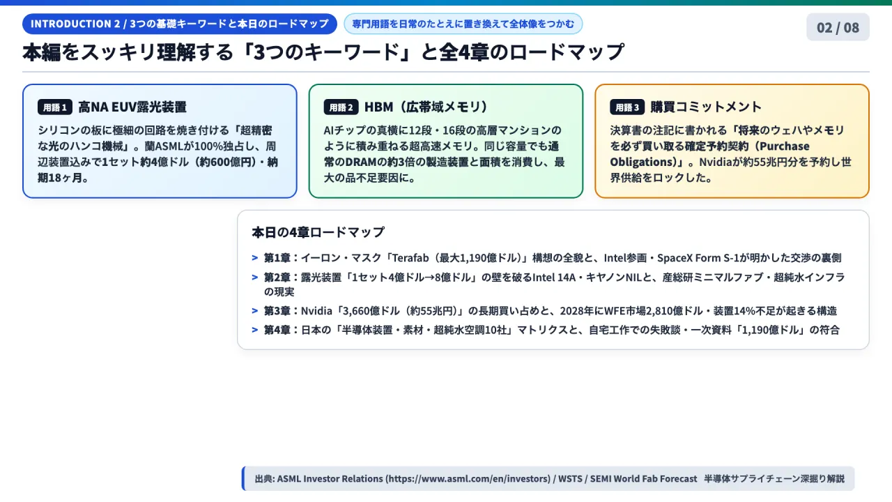
- High-NA EUV Lithography (0.55 NA): ASML’s EXE:5000 and EXE:5200 increase numerical aperture from 0.33 to 0.55, enabling single-exposure printing of sub-2nm features. A scanner connected to Tokyo Electron track coaters, developers, inspection tools, and vacuum robotics forms a single patterning module costing approximately $400 million (60 billion yen) with an 18-month lead time.
- High Bandwidth Memory (HBM): Advanced GPUs require immense bandwidth to prevent processor stalls. HBM stacks 12 to 16 DRAM dies vertically using through-silicon vias (TSVs) micro-bumped onto an interposer. Because thinning, etching, stacking, and testing incur compound yield penalties, producing one gigabit of HBM consumes roughly 3x the wafer fab equipment and cleanroom footprint of standard DDR5 DRAM.
- Purchase Obligations: Disclosed in footnotes to Form 10-K and 10-Q under Commitments and Contingencies, these binding contracts commit buyers to purchase wafers, components, and packaging over one to five years, revealing which hyperscalers have locked global capacity.
2. Terafab Architecture and SpaceX Form S-1 Disclosures
In March 2026, SpaceX and Tesla unveiled TeraFab AI, LLC, followed in April 2026 by Intel joining as technology partner.
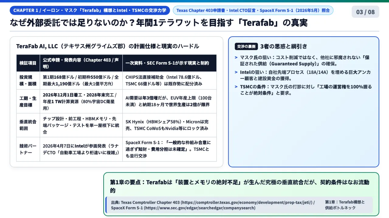
Texas Chapter 403 JETI filings define the parameters for the Grimes County site near Austin:
| Architectural Metric | Public Specification | Operational Significance |
|---|---|---|
| Site & Entity | TeraFab AI, LLC (Grimes County, TX) | Cluster near Giga Texas with on-site gas power and water treatment |
| Facility Footprint | Up to 100 Million Square Feet | Roughly 200 times the footprint of Tokyo Dome across all phases |
| Initial Phase CapEx | $16.8 Billion | Foundational fab infrastructure and cleanroom shell construction |
| Initial Scope & Ceiling | ~$55.0B Scope / Up to $119.0B Max | Phase 1-2 tooling up to total cumulative capital ceiling |
| Construction Schedule | Groundbreaking: Dec 1, 2026; Op: Late 2028 | Accelerated two-year timetable to achieve initial wafer output |
| Target Output | 1 Terawatt (10^12 W) Compute / Year | ~80% to SpaceX orbital data satellites; ~20% to Tesla FSD and Optimus |
| Vertical Integration | Single-Roof In-House Execution | Unifying logic design, wafer fab, HBM stacking, 3D packaging, and testing |
With SK Hynix holding 58% of HBM and TSMC’s CoWoS lines booked through 2027 by NVIDIA and Apple, latecomers face severe rationing. Terafab seeks guaranteed compute delivery independent of competitor allocations.
Intel CTO Pushkar Ranade noted that building a fab involves hundreds of sequential chemical reactions and atomic-scale manipulations that cannot be bootstrapped without mature recipes and fab operational expertise. While Intel needs volume demand, SpaceX’s Form S-1 filed in May 2026 reveals three sober qualifications:
- Non-Binding Framework: The agreement remains a General Framework with IP rights and capital-cost sharing ratios still under negotiation.
- TSMC Operational Governance Deadlock: Musk previously engaged TSMC, but TSMC insisted on 100% operational governance, which Musk rejected.
- CHIPS Act Exhaustion: Federal grants were pre-allocated to Intel ($7.86B), TSMC ($6.60B), Micron ($6.10B), and Samsung ($4.75B), leaving Terafab dependent on Texas Chapter 403 property tax abatements.
3. Escalating Lithography Costs and Alternative Paradigms
Advanced fab costs double every four to five years, now exceeding $20 billion per facility:
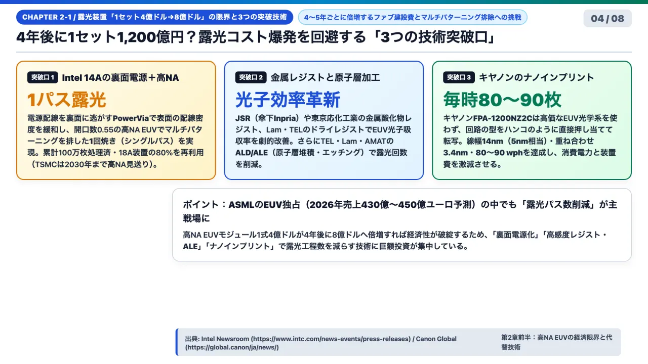
A single High-NA EUV patterning module costs $400 million today and threatens to reach $800 million by 2030, challenging commercial viability. Three technical pathways bypass this escalation:
- Intel 14A Backside Power (PowerVia) and Single-Pass High-NA EUV: Under low-NA EUV (0.33 NA), sub-2nm features require multi-patterning, multiplying EUV passes, mask costs, and overlay defects. Intel’s 14A node (2028) routes power supply lines to the rear of the wafer via PowerVia, clearing front-side routing congestion and enabling single-pass exposures with High-NA EUV. Intel processed over 1 million test wafers while reusing roughly 80% of 18A fab tooling. Conversely, TSMC is retaining 0.33 NA multi-patterning for N2, A16, and A14 through roughly 2030.
- Metal-Oxide Resists and Atomic Layer Engineering: To maximize photon absorption from $400 million scanners, JSR (Inpria) and Tokyo Ohka Kogyo (4186) commercialized tin-based metal-oxide photoresists (MOx). Tokyo Electron (8035) and Lam Research deployed dry-resist vapor deposition alongside atomic layer deposition (ALD) and atomic layer etching (ALE), transferring patterning precision to chemical surface engineering.
- Canon Nanoimprint Lithography (FPA-1200NZ2C): Rather than using optical projection mirrors, Canon (7751) presses patterned masks directly into liquid resist. Achieving 14nm half-pitch (5nm logic equivalent), 3.4nm overlay, and 80 to 90 wph throughput, it consumes 10% of EUV power and eliminates laser plasma sources, cutting costs for 3D NAND and packaging.
4. Cleanroom Dogma: AIST Minimal Fab and Infrastructure Constraints
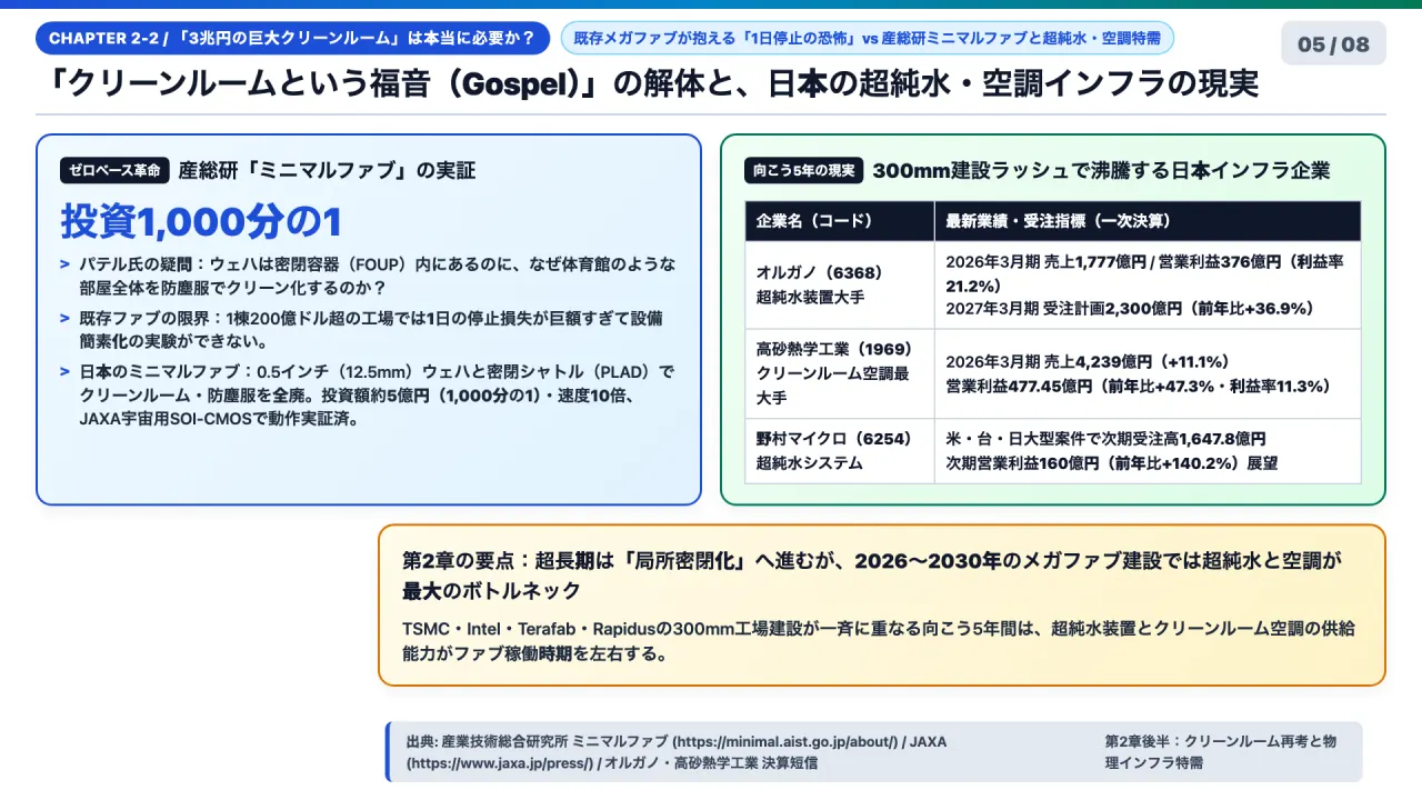
Intel executives acknowledged that ballroom cleanrooms are legacy dogma: modern wafers travel inside sealed Front Opening Unified Pods (FOUPs). Yet when a single fab represents $20 billion and a single day of downtime causes tens of millions of dollars in losses, operators avoid altering cleanroom standards.
Japan’s National Institute of Advanced Industrial Science and Technology (AIST) challenged this model with Minimal Fab:
- Architecture: Uses 0.5-inch (12.5mm) silicon wafers enclosed in localized Minimal Shuttles docked via Plasma Lock Systems (PLAD), eliminating cleanrooms entirely.
- Economics: Cuts tool line investment by 1,000x to roughly $3.3 million (500 million yen), accelerates cycle times by 10x, and proved orbital flight heritage with JAXA radiation-hardened SOI-CMOS chips.
However, all megagabs built through 2030 (Terafab, TSMC, Intel, Rapidus) remain standard 300mm cleanroom facilities, making facility infrastructure the primary operational constraint:
- Organo (6368): Ultrapure water (UPW) systems provider. FY2026 revenue reached 177.7 billion yen (+9.5%), operating profit rose 21.0% to 37.6 billion yen (21.2% margin), and FY2027 orders target 230 billion yen (+36.9%).
- Takasago Thermal Engineering (1969): Cleanroom HVAC leader. FY2026 revenue hit 423.9 billion yen (+11.1%), with operating income rising 47.3% to 47.7 billion yen.
- Nomura Micro Science (6254): Projecting 164.8 billion yen in orders and 16.0 billion yen in operating profit (+140.2%) from U.S. and Asian fabs.
5. NVIDIA’s $366B Supply Lock and the 14% Equipment Shortfall
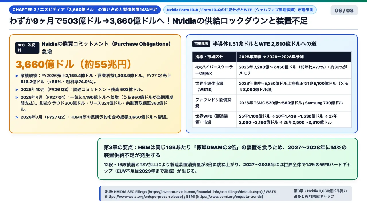
Capital expenditures across Microsoft, Amazon, Google, and Meta will hit $720 billion to $745 billion in 2026 (+77% YoY), with 30% allocated to high-performance memory. NVIDIA captured this expansion, generating FY2026 revenue of $215.9 billion and Q1 FY2027 quarterly revenue of $81.6 billion (74.9% gross margin).
Footnotes in NVIDIA’s Form 10-Q track rapid capacity preemption:
- October 2025 (Q3 FY26): $50.3 billion in purchase obligations.
- April 2026 (Q1 FY27): $119.0 billion (+137% in six months), with $95.0 billion due within 12 months.
- July 2026 (Q2 FY27): Surged to $366.0 billion to lock HBM4, advanced substrate capacity, and wafer allocations across SK Hynix, Micron, and TSMC.
WSTS revised the 2026 global semiconductor market upward by $535 billion to $1.51 trillion (+93% YoY), with memory exceeding $800 billion. Because HBM requires 3x the equipment of standard DRAM, global WFE spending will expand from $116.9 billion in 2025 to $281.0 billion in 2028, generating a structural 14% equipment hardware shortfall with EUV deficits extending to 2029.
6. Japan’s 10 Chokepoint Suppliers and Structural Observations
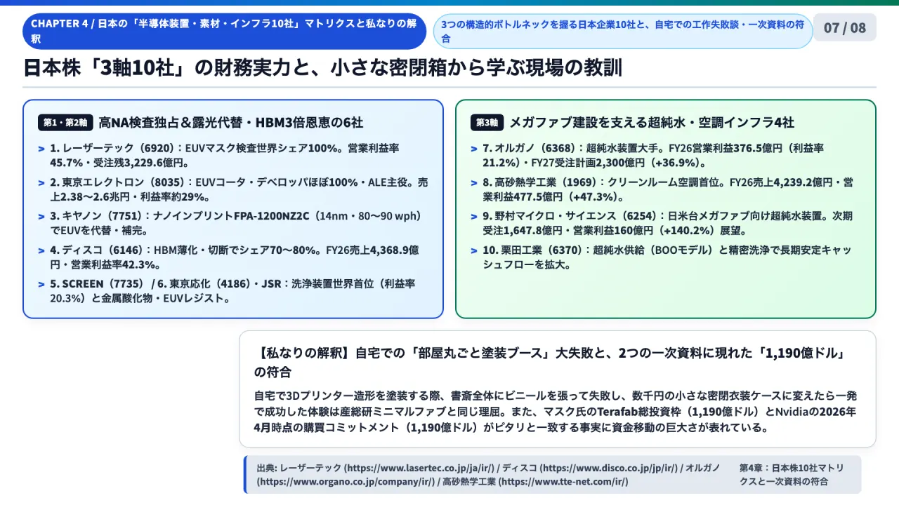
Ten Japanese equipment, materials, and infrastructure suppliers control critical chokepoints:
- Lasertec (6920): Holds a 100% global monopoly on actinic EUV photomask inspection operating at 13.5nm. Under Intel’s 14A single-pass design, a single mask defect ruins entire wafer runs. Guided FY2026 operating profit of 105.0 billion yen (45.7% margin) against a 323.0 billion yen backlog.
- Tokyo Electron (8035): Commands ~90% global share in EUV coater/developer tracks, leading in atomic layer etching and wafer bonders.
- Canon (7751): Deploying nanoimprint lithography (FPA-1200NZ2C) and back-end lithography systems.
- Disco (6146): Controls 70% to 80% global share in precision grinders and dicers essential for 12-to-16-layer HBM stacks. FY2026 operating profit hit 184.9 billion yen (42.3% margin).
- SCREEN Holdings (7735): Global leader in single-wafer wet cleaning systems (20.3% operating margin).
- Tokyo Ohka Kogyo (4186) & JSR: Dominant suppliers of EUV photoresists and metal-oxide formulations.
- Organo (6368): Ultrapure water systems provider; FY2027 orders forecast at 230 billion yen (+36.9%).
- Takasago Thermal Engineering (1969): Industrial cleanroom HVAC contractor; FY2026 operating profit rose 47.3% to 47.7 billion yen.
- Nomura Micro Science (6254): High-purity water systems for overseas fabs; targeting 16.0 billion yen in operating profit (+140.2%).
- Kurita Water Industries (6370): Expanding recurring-revenue Build-Own-Operate (BOO) ultrapure water contracts.
The Personal Scale Anecdote
This cleanroom inertia mirrors a personal experience. Preparing to spray-paint a 3D-printed prototype part with a mirror finish, I attempted to convert an entire home study into a cleanroom with taped plastic sheeting, full protective suits, and two air purifiers at maximum power.
Walking across the room generated static, circulating clothing fibers that ruined the wet paint, while adhesive tape damaged the wallpaper upon removal.
A scale-modeling colleague resolved the problem: purchase a $30 clear plastic storage tub, cut two arm holes fitted with sealed rubber gloves, and spray the part inside that small container. The part dried flawlessly inside a normal room.
AIST’s Minimal Fab applied this insight industrially with 12.5mm wafers in sealed shuttles, yet the global industry remains bound to $20 billion cleanrooms because legacy yield models cannot tolerate deviation.
The $119 Billion Coincidence
A compelling financial symmetry connects these dockets: the total phased investment ceiling for Elon Musk’s Terafab in Grimes County is $119.0 billion.
In its April 2026 Form 10-Q filing, NVIDIA’s total purchase commitments to external foundries and memory suppliers stood at exactly $119.0 billion before reaching $366.0 billion. NVIDIA’s capital commitment to lock outsourced production equals the total capital required to construct the world’s largest semiconductor complex from raw land.
7. Actionable Decision Framework for Technology Leaders and Investors
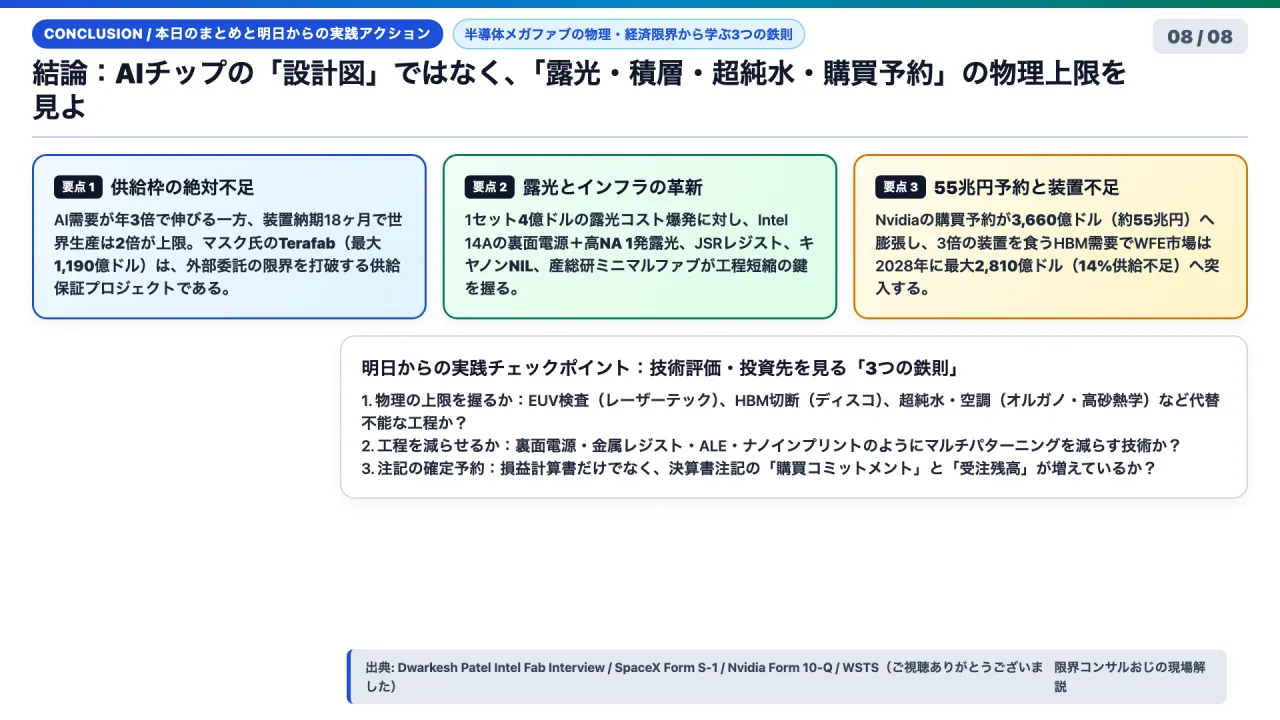
- Audit Tool Delivery Lead Times Over Silicon Roadmaps: When evaluating processor supply security, verify supplier tool delivery lead times (averaging 18 months) and vendor concentration rather than theoretical processor benchmarks. Pricing power resides with physical chokepoints: Lasertec in mask inspection, Disco in wafer dicing, and Organo in UPW systems.
- Track Alternative Process Simplification Adoption: Monitor quarterly yield progress and commercial adoption across three bypass vectors: Intel 14A single-pass PowerVia execution, metal-oxide resist integration, and Canon nanoimprint commercial deployments in memory and packaging layers.
- Cross-Reference Purchase Commitments Against Tool Backlogs: Reconcile customer purchase obligations in SEC Form 10-Q reports against equipment backlogs at Tokyo Electron, Disco, and Organo. Discrepancies between hyperscaler commitments and physical tool deliveries provide the most reliable leading indicator of real-world compute supply.
Primary Sources and References
- Intel Fab D1X Technical Investigation and CTO Interview:
- TeraFab AI, LLC Regulatory Filings & SpaceX SEC S-1:
- NVIDIA Financial Reports and Purchase Obligations:
- Lithography and Semiconductor Market Data:
- ASML Holding N.V.: High-NA EUV (EXE:5000/5200) Technical Specifications
- Canon Global: FPA-1200NZ2C Nanoimprint Semiconductor Lithography System
- Intel Corporation: Intel 14A Node and PowerVia Architecture Announcements
- World Semiconductor Trade Statistics (WSTS): Global Semiconductor Market Forecast Updates
- SEMI: World Fab Forecast and Wafer Fab Equipment Projections
- Minimal Fab and Japanese Supplier Disclosures:
- National Institute of Advanced Industrial Science and Technology (AIST): Minimal Fab Development Consortium
- Japan Aerospace Exploration Agency (JAXA): Orbital Demonstration of Minimal Fab SOI-CMOS
- Lasertec Corporation Investor Relations (6920)
- Disco Corporation Investor Relations (6146)
- Organo Corporation Investor Relations (6368)
- Takasago Thermal Engineering Co., Ltd. Investor Relations (1969)